Doping Technology for outstanding OLED
Conventional Technology
Conventional OLEDs are limited to thin transport layers and special electrode materials and/or pre-treatment due to the following restrictions:
- The conductivity of the charge carrier transport layers is low, leading to ohmic losses.
- The injection of charge carriers from the electrodes into the transport layers has a high barrier, leading to an additional driving voltage increase.
Advantages of Novaled PIN OLED® Doping Technology
The organic stack of doped and undoped OLEDs is similar. In contrast to conventional OLEDs, Novaled PIN OLED® technology introduces an additional degree of freedom for product design, considerably enhancing hole and electron-transport as well as charge carrier injection. As a result of doping, additional process steps, such as ITO treatment, are not needed.
In addition, when using p- and n-doping, a much wider range of materials can be used for the anode and cathode. As a result, OLEDs produced using Novaled PIN OLED® technology have a very low driving voltage and high substrate compatibility, while maintaining high power efficiency and long lifetime.
Novaled has developed several doping and transport materials that can be used in OLEDs or OSCs to further enhance and support the advantages of its doping technology. A wide range of interlayers and emitter materials can be integrated easily into Novaled's PIN structure.
The success of Novaled's technology and materials speaks for itself as major manufacturers use Novaled technology and materials in the mass production of their OLED display products, and might use Novaled technology and materials in future OLED lighting products.
Beyond Limits
Taking OLEDs to Unexplored Frontiers
Novaled’s doping technology and materials enable high power efficiency and long lifetime OLED devices. They result in fewer processing steps and an additional degree of freedom for product design.
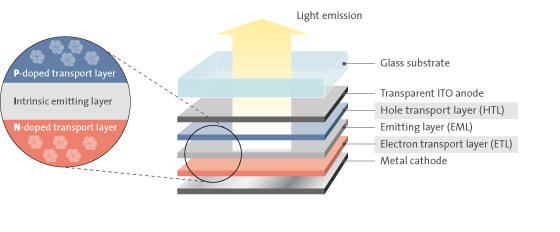
Working Principle of Novaled's Doping Technology
- Holes are injected by the anode and transported by the p-doped hole transport layer (p-HTL) to the emissive layer (EML).
- Electrons are injected by the cathode and transported by the n-doped electron transport layer (n-ETL).
- Recombination of the charge carriers takes place in the EML and light is emitted.
- Dopant and host materials for the p-HTL and the n-ETL are provided by Novaled.